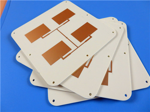
Advanced 8-Layer HDI RF PCB Solution with RO4350B Core and RO4450F Bondply
1.Introduction to Our Premium RF PCB Technology
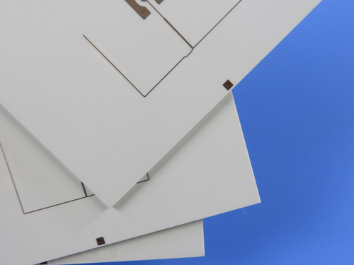
At the forefront of high-frequency PCB innovation, our 8-layer HDI RF printed circuit board combines Rogers RO4350B high-frequency laminate with RO4450F bondply to deliver exceptional performance for demanding RF applications. This advanced PCB solution is engineered for 5G infrastructure, automotive radar systems, satellite communications, and RF identification technologies.
2.Cutting-Edge Material Technology
RO4350B Core Material Advantages:
Superior high-frequency performance with dielectric constant (Dk) of 3.48±0.05 at 10GHz
Ultra-low signal loss (dissipation factor of 0.0037 at 10GHz)
Excellent thermal management (0.69 W/m/K conductivity)
Outstanding dimensional stability (CTE: X=10, Y=12, Z=32 ppm/°C)
High temperature resistance (>280°C Tg)
Cost-effective alternative to traditional PTFE materials
UL 94 V-0 flammability rating for safety-critical applications
RO4450F Bondply Features:
Optimized for multilayer RF designs (Dk: 3.52±0.05 at 10GHz)
Enhanced lamination capability (0.004 dissipation factor)
Superior thermal performance (0.65 W/m/K conductivity)
Excellent CTE characteristics (X=19, Y=17, Z=50 ppm/°C)
Compatible with sequential lamination processes
Improved flow characteristics for void-free construction
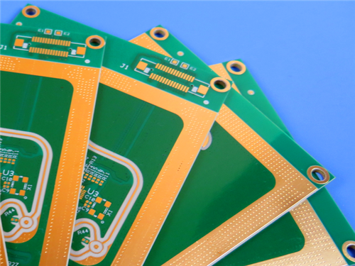
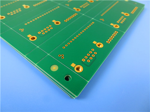
3.PCB Construction Details
| Attribute | Details |
|---|
| Base Material | RO4350B |
| Layer Count | 8 layers |
| Board Dimensions | 96.4 mm x 163.9 mm (± 0.15 mm) |
| Minimum Trace/Space | 4/6 mils |
| Minimum Hole Size | 0.4 mm |
| Blind Vias | GTL-L7, L3-GBL, GTL-L2, L7-GBL, GTL-L3, GTL-L4, GTL-L5, L5-GBL, L4-GBL, GTL-L6, L6-GBL, L2-GBL, mechanical drill |
| Finished Board Thickness | 1.8 mm |
| Finished Copper Weight | Outer layers: 1 oz (1.4 mils) Inner layers: 1 oz (1.4 mil) / 0.5 oz (0.7 mil) |
| Via Plating Thickness | 20 μm |
| Surface Finish | Electroless Nickel Immersion Gold |
| Top Silkscreen | White |
| Bottom Silkscreen | White |
| Top Solder Mask | Green |
| Bottom Solder Mask | Green |
| Via Treatment | All vias resin filled and capped |
| Quality Assurance | 100% Electrical test prior to shipment |
| Impedance Control | 50 ohm on GTL 9.4 mil, reference layer 2 50 ohm on L2 7 mil, reference layer GTL, L3/GND 50 ohm on L7 7 mil, reference layer L6/PWR, L8/GBL 50 ohm on GBL 9.4 mil, reference layer L7/GND |
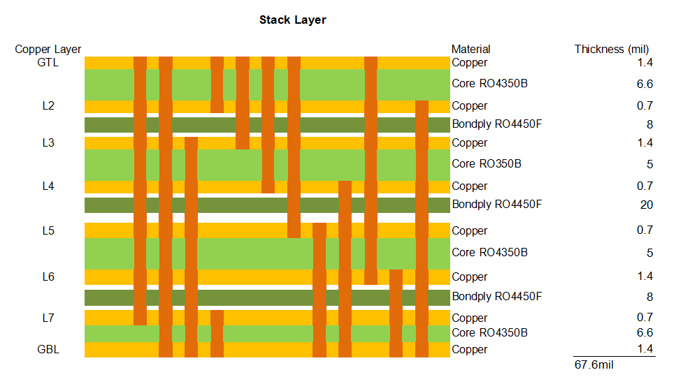
4.Optimized Layer Stackup Architecture
Our carefully engineered 8-layer stackup delivers maximum performance:
| Layer | Material | Thickness |
|---|
| Layer 1 | Copper + plating | 17 μm |
| Core 1 | Rogers RO4350B | 0.168 mm (6.6 mil) |
| Layer 2 | Copper | 17 μm |
| Bondply 1 | RO4450F | 8 mil |
| Layer 3 | Copper | 35 μm |
| Core 2 | Rogers RO4350B | 0.127 mm (5 mil) |
| Layer 4 | Copper | 17 μm |
| Bondply 2 | RO4450F | 20 mil |
| Layer 5 | Copper | 17 μm |
| Core 3 | Rogers RO4350B | 0.127 mm (5 mil) |
| Layer 6 | Copper | 35 μm |
| Bondply 3 | RO4450F | 8 mil |
| Layer 7 | Copper | 17 μm |
| Core 4 | Rogers RO4350B | 0.168 mm (6.6 mil) |
| Layer 8 | Copper + plating | 17 μm |
5.Comprehensive PCB Statistics
Component Density: 76 total components
Pad Configuration:
Total pads: 303
Thru-hole pads: 117
SMT pads: 186 (121 top, 65 bottom)
Via Count: 335 vias
Net Count: 6 nets
6.Accepted Standards
Artwork Format: Gerber RS-274-X
Quality Standard: IPC-Class-2 compliant
Availability: Worldwide production and shipping
7.Target Applications
5G Infrastructure: Base station antennas and power amplifiers
Automotive Electronics: Radar systems and sensors
Aerospace & Defense: Satellite communication LNBs
RFID Systems: High-performance identification tags
Microwave Systems: Direct broadcast satellite components
8.Why Choose Our RF PCB Solution?
1.Superior Signal Integrity: Tight impedance control and low-loss materials
2.Enhanced Reliability: Robust construction with resin-filled vias
3.Thermal Performance: Excellent heat dissipation characteristics
4.Manufacturing Consistency: Strict IPC-Class-2 quality standards
5.Technical Support: Expert guidance for your specific application needs
This high-performance RF PCB solution represents the perfect combination of advanced materials science and precision engineering, delivering the exceptional quality needed for today's most demanding high-frequency applications. Contact our technical team today to discuss how this technology can benefit your next RF project.
|